
Silicon Controlled Rectifier
Silicon Controlled Rectifier
We know that the diode allows electric current in one direction and blocks electric current in another direction. In other words, the diode converts the AC current in to DC current. This unique behavior of the diodes makes it possible to build different types of rectifiers such as half wave, full wave and bridge rectifiers. These rectifiers converts the Alternating Current into Direct Current.
The half wave, full wave, and bridge rectifiers uses normal p-n junction diodes (two layer diodes). So if the voltage applied to these diodes is high enough, then the diodes may get destroyed. So the rectifiers cannot operate at high voltages.
To overcome these drawback, scientists have developed a special type of rectifier known as Silicon Controlled Rectifier. These rectifiers can withstand at high voltages.
Silicon Controlled Rectifier Definition
A Silicon Controlled Rectifier is a 3 terminal and 4 layer semiconductor current controlling device. It is mainly used in the devices for the control of high power. Silicon controlled rectifier is also sometimes referred to as SCR diode, 4-layer diode, 4-layer device, or Thyristor. It is made up of a silicon material which controls high power and converts high AC current into DC current (rectification). Hence, it is named as silicon controlled rectifier.
What is Silicon Controlled Rectifier?
Silicon controlled rectifier is a unidirectional current controlling device. Just like a normal p-n junction diode, it allows electric current in only one direction and blocks electric current in another direction. A normal p-n junction diode is made of two semiconductor layers namely P-type and N-type. However, a SCR diode is made of 4 semiconductor layers of alternating P and N type materials.

The principle of p-n-p-n switching was developed by Tanenbaum, Goldey, Moll and Holonyak of Bell Laboratories in 1956. The silicon controlled rectifier was developed by a team of power engineers led by Gordon Hall and commercialized by Frank W. Frank W. "Bill" Gutzwiller in 1957. In the early days of this device development, it is often referred by names like SCR and controlled rectifier. However, now-a-days, this device is often referred by Thyristor.
Silicon controlled rectifiers are used in power control applications such as power delivered to electric motors, relay controls or induction heating elements where the power delivered has to be controlled.
Silicon Controlled Rectifier Symbol
The schematic symbol of a silicon controlled rectifier is shown in the below figure. A SCR diode consists of three terminals namely anode (A), cathode (K), Gate (G). The diode arrow represents the direction of conventional current.

Construction of Silicon Controlled Rectifier
A silicon controlled rectifier is made up of 4 semiconductor layers of alternating P and N type materials, which forms NPNP or PNPN structures. It has three P-N junctions namely J1, J2, J3 with three terminals attached to the semiconductors materials namely anode (A), cathode (K), and gate (G). Anode is a positively charged electrode through which the conventional current enters into an electrical device, cathode is a negatively charged electrode through which the conventional current leaves an electrical device, gate is a terminal that controls the flow of current between anode and cathode. The gate terminal is also sometimes referred to as control terminal.
The anode terminal of SCR diode is connected to the first p-type material of a PNPN structure, cathode terminal is connected to the last n-type material, and gate terminal is connected to the second p-type material of a PNPN structure which is nearest to the cathode.
In silicon controlled rectifier, silicon is used as an intrinsic semiconductor. When pentavalent impurities are added to this intrinsic semiconductor, an N-type semiconductor is formed. When trivalent impurities are added to an intrinsic semiconductor, a p-type semiconductor is formed.
When 4 semiconductor layers of alternating P and N type materials are placed one over another, three junctions are formed in PNPN structure. In a PNPN structure, the junction J1 is formed between the first P-N layer, the junction J2 is formed between the N-P layer and the junction J3 is formed between the last P-N layer. The doping of PNPN structure is depends on the application of SCR diode
Modes of Operation in SCR
There are three modes of operation for a Silicon Controlled Rectifier (SCR), depending upon the biasing given to it.
1) Forward Blocking Mode (Off State)
2) Forward Conducting Mode (On State)
3) Reverse Blocking Mode (Off State)
1) Forward Blocking Mode (Off State)
In this mode of operation, the positive voltage (+) is given to anode A (+), negative voltage (-) is given to cathode K (-), and gate G is open circuited as shown in the below figure. In this case, the junction J1 and junction J3 are forward biased whereas the junction J2 becomes reverse biased. Due to the reverse bias voltage, the width of depletion region increases at junction J2. This depletion region at junction J2 acts as a wall or obstacle between the junction J1 and junction J3. It blocks the current flowing between junction J1 and junction J3. Therefore, the majority of the current does not flow between junction J1 and junction J3. However, a small amount of leakage current flows between junction J1 and junction J3.

When the voltage applied to the SCR reaches a breakdown value, the high energy minority carriers causes avalanche breakdown. At this breakdown voltage, current starts flowing through the SCR. But below this breakdown voltage, the SCR offers very high resistance to the current and so it will be in off state.
In this mode of operation, SCR is forward biased but still current does flows through it. Hence, it is named as Forward Blocking Mode.
2) Forward Conducting Mode (On State)
The Silicon Controlled Rectifier can be made to conduct in two ways:
- By increasing the forward bias voltage applied between anode and cathode beyond the breakdown voltage
- By applying positive voltage at gate terminal.
In the first case, the forward bias voltage applied between anode and cathode is increased beyond the breakdown voltage, the minority carriers (free electrons in anode and holes in cathode) gains large amount of energy and accelerated to greater velocities. This high speed minority carriers collides with other atoms and generates more charge carriers. Likewise, many collisions happens with other atoms. Due to this, millions of charge carriers are generated. As a result depletion region breakdown occurs at junction J2 and current starts flowing through the SCR. So the SCR will be in On state. The current flow in the SCR increases rapidly after junction breakdown occurs.

In the second case, a small positive voltage VG is applied to the gate terminal. As we know that, in forward blocking mode, current does not flows through the circuit because of the wide depletion region present at the junction J2. This depletion region was formed because of the reverse biased gate terminal. So this problem can be easily solved by applying a small positive voltage at the Gate terminal. When a small positive voltage is applied to the gate terminal, it will become forward biased. So the depletion region width at junction J2 becomes very narrow. Under this condition, applying a small forward bias voltage between anode and cathode is enough for electric current to penetrate through this narrow depletion region. Therefore, electric current starts flowing through the SCR circuit.
In second case, we no need to apply large voltage between anode and cathode. A small voltage between anode and cathode, and positive voltage to gate terminal is enough to brought SCR from blocking mode to conducting mode.
In this mode of operation, SCR is forward biased and current flows through it. Hence, it is named as Forward Conducting Mode.
3) Reverse Blocking Mode (On State)
In this mode of operation, the negative voltage (-) is given to anode (+), positive voltage (+) is given to cathode (-), and gate is open circuited as shown in the below figure. In this case, the junction J1 and junction J3 are reverse biased whereas the junction J2 becomes forward biased.

As the junctions J1 and junction J3 are reverse biased, no current flows through the SCR circuit. But a small leakage current flows due to drift of charge carriers in the forward biased junction J2. This small leakage current is not enough to turn on the SCR. So the SCR will be in Off state.
V-I Characteristics of SCR
The V-I characteristics of SCR is shown in the below figure. The horizontal line in the below figure represents the amount of voltage applied across the SCR whereas the vertical line represents the amount of current flows in the SCR.
VA = Anode voltage, IA = Anode current, +VA = Forward anode voltage, +IA = Forward anode current, -VA = Reverse anode voltage, +IA = Reverse anode current
The V-I characteristics of SCR is divided into three regions:
- Forward blocking region
- Forward conduction region
- Reverse blocking region
- Forward blocking region
In this region, the positive voltage (+) is given to anode (+), negative voltage (-) is given to cathode (-), and gate is open circuited. Due to this the junction J1 and J3 become forward biased while J2 become reverse biased. Therefore, a small leakage current flows from anode to cathode terminals of the SCR. This small leakage current is known as forward leakage current.

The region OA of V-I characteristics is known as forward blocking region in which the SCR does not conduct electric current.
- Forward Conduction region
If the forward bias voltage applied between anode and cathode is increased beyond the breakdown voltage, the minority carriers (free electrons in anode and holes in cathode) gains large amount of energy and accelerated to greater velocities. This high speed minority carriers collides with other atoms and generates more charge carriers. Likewise, many collisions happens with atoms. Due to this, millions of charge carriers are generated. As a result depletion region breakdown occurs at junction J2 and current starts flowing through the SCR. So the SCR will be in On state. The current flow in the SCR increases rapidly after junction breakdown occurs.
The voltage at which the junction J2 gets broken when the gate is open is called forward breakdown voltage (VBF).
The region BC of the V-I characteristics is called conduction region. In this region, the current flowing from anode to cathode increases rapidly. The region AB indicates that as soon as the device becomes on, the voltage across the SCR drops to some volts.
- Reverse Blocking Region
In this region, the negative voltage (-) is given to anode (+), positive voltage (+) is given to cathode (-), and gate is open circuited. In this case, the junction J1 and junction J3 are reverse biased whereas the junction J2 becomes forward biased.
As the junctions J1 and junction J3 are reverse biased, no current flows through the SCR circuit. But a small leakage current flows due to drift of charge carriers in the forward biased junction J2. This small leakage current is called reverse leakage current. This small leakage current is not sufficient to turn on the SCR.
If the reverse bias voltage applied between anode and cathode is increased beyond the reverse breakdown voltage (VBR), an avalanche breakdown occurs. As a result, the current increases rapidly. The region EF is called reverse avalanche region. This rapid increase in current may damage the SCR device.
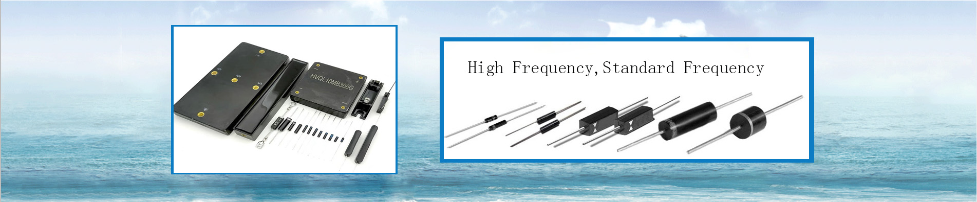
For more information, PLEASE visits our Web site: www.tomdiode.com
Latest News
Latest News
Contact Us

Global Marketing: Sales team
E-mail: [email protected]
E-mail: [email protected]
Skype: tomdiode


 Skype Chat
 Mail inquiry